Two variants of Intel's Xeon processors are employed presently in HPC systems (clusters as well as integrated systems): The Nehalem EX, officially the X7500 chip series, and the Westmere EP, officially the X5600 series. Although there is a great deal of communality they are sufficiently different to discuss both processors separately.
Nehalem EX
The Nehalem EX came available in March 2010 or, more officially, the X7500 series of processors can be regarded as a heavy-duty server extension of the earlier Nehalem EP (X5500) processor. As such it has double the amount of cores, eight, and the number of QPI links also doubled to four to enable the connection to other processors on a server board. In addition the bandwidth is raised because the number of memory interfaces has increased from three to four. As the bandwidth per memory channel is 10.833 GB/s the aggregate bandwidth of the chip is 43.3 MB/s. The Nehalem EX is employed in SGI's Altix UV systems and a variety of products from cluster vendors. Below we show the block diagram of the processor core which in fact identical to that of the Nehalem EP and built in the same 45 nm technology. A block diagram of the core is given in Figure 17.
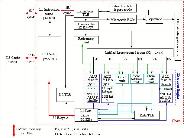
Figure 17: Block diagram of the Intel Nehalem processor.
while the layout of an 8-core chip is shown in Figure 18
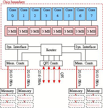
Figure 18: Diagram of a Nehalem EX processor.
To stay backwards compatible with the x86 (IA-32) Instruction Set Architecture which comprises a CISC instruction set Intel developed a modus in which these instructions are split in so-called micro operations (µ-ops) of fixed length that can be treated in the way RISC processors do. In fact the µ-ops constitute a RISC operation set. The price to be payed for this much more efficient instruction set is an extra decoding stage. Branch prediction has been improved and also a second level TLB cache been added.
As in the earlier Core architecture 4 µ-ops/cycle and some macro-instructions as well as some µ-ops can be fused, resulting in less instruction handling, easier scheduling and better instruction throughput because these fused operations can be executed in a single cycle. In the Nehalem 2 additional µ-ops can be fused in comparison to the Core architecture.
As can be seen in Figure 17 the processor cores have an execution trace cache which holds partly decoded instructions of former execution traces that can be drawn upon, thus foregoing the instruction decode phase that might produce holes in the instruction pipeline. The allocator dispatches the decoded instructions, the µ-ops, to the unified reservation station that can issue up to 6 µ-ops/cycle to the execution units, collectively called the Execution Engine. Up to 128 µ-ops can be in flight at any time. Figure 17 shows that port 0 and port 5 drive two identical Integer ALUs as well as Integer SSE units. Port 0, 1, and 5 take care of the various floating-point operations.
The two integer Arithmetic/Logical Units at port 0 and 5 are kept simple in order to be able to run them at twice the clock speed. In addition there is an ALU at port 1 for complex integer operations that cannot be executed within one cycle. The floating-point units contain also additional units that execute the Streaming SIMD Extensions 4 (SSE4) repertoire of instructions, an instruction set of more than 190 instructions, that initially was meant for vector-oriented operations like those in multimedia, and 3-D visualisation applications but also is of advantage for regular vector operations as occur in dense linear algebra. The length of the operands for these units is 128 bits. The Intel compilers have the ability to address the SSE4 units. This enables in principle much higher floating-point performance. Port 2, 3, and 4 serve the Load unit the Store Address unit, and the Store Data unit, respectively.
A notable enhancement that cannot be shown in the figures is that the Nehalem (again) supports multi-threading much in the style of IBM's simultaneous multithreading and called Hyperthreading by Intel. Hyperthreading was earlier introduced in the Pentium 4 but disappeared in later Intel processors because the performance gain was very low. Now with a much higher bandwidth and larger caches speedups of more than 30% for some codes have been observed with Hyperthreading. Another feature that cannot be shown is thew so-called Turbo Mode. This meaans that the clock cycle can be raised from its nominal speed (2.91 GHz for the fastest variant) by steps of 133 MHz to over 3 GHz as long as the thermal envelope of the chip is not exceeded. So, when some cores are relatively idle other cores can take advantage by operating at a higher clock speed.
The L1 caches have the same size as in the Nehalem's predecessor but the L2 cache is much smaller: 256 KB instead of 6 MB. It is much faster however and able to deliver requested data in 10 cycles or less. The Nehalems feature a common L3 cache that is used by all eight cores in the EX version. Each core has its own section of 3 MB but when data is not found in the section of a core the other sections can be searched for the missing data item(s). The L3 cache is inclusive which means that it contains all data that are in the L2 and L1 cache. The consequence is that when a data item cannot be found in the L3 cache it is also not in any of the caches of the other cores and one therefore need not search them.
In Figure 18 it can be noticed that apart from the first bank of memory of ≤ 32 GB also a second and third bank are depicted, represented by dashed boxes. This means that it is indeed possible to have up to 96 GB of memory/processor. However, this can only be done at the expense of the memory bus speed: for one bank it is 1333 MB/s, for two banks it is 1066 MB/s, and for three banks only 800 MB/s. So, the latter two options may be chosen for instance for database systems that benefit from a large memory that not needs to be at the very highest speed. For HPC purposes, however, configurations with only one memory bank/processor will usually be offered.
Westmere EP
The Westmere EP (X5600 series) is a 32 nm technology shrink of the Nehalem EP chip. The smaller feature size is used to place 6 cores on a die. The fastest variant, the X5690 has a clock cycle of 3.46 GHz at 130 W. The structure of the core is the same as in the Nehalem processors (see Figure 19 but there are slight differences in the instruction set for the Advanced Encryption Standard (AES). The new instructions, among which a carry-less multiplication are said to speed up the en/decryption rate by a factor of three. Also the Westmere EP supports the use of 1 GB pages. The packaging on the chip is, apart from the number of cores, identical to that of the Nehalem EP chip with exception of the shared L3 cache. The size of this is halved from 24 MB to 12MB. The chip layout is depicted in Figure 19.
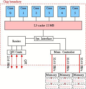
Figure 19: Diagram of a Westmere processor.