Since slightly more than a year two BlueGene types of systems have become available: the BlueGene/L and the BlueGene/P, the successor of the former. Both feature processors based on the PowerPC 400 processor family.
The BlueGene/L processor
This processor is in fact a modified PowerPC 440 processor, which is made especially for the IBM BlueGene family. It runs presently at a speed of 700 MHz. The modification lies in tacking on floating-point units (FPUs)that are not part of the standard processor but can be connected to the 440's APU bus. Each FPU contains two floating-point functional units capable of performing 64-bit multiply-adds, divisions and square-roots. Consequently, the theoretical peak performance of a processor core is 2.8 Gflop/s. Figure 15. shows the embedding of two processor cores on a chip.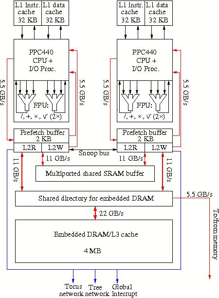
Figure 15: Block diagram of an IBM BlueGene/L processor chip.
As can be seen from the figure the L2 cache is very small: only 2 KB divided in a read and a write part. In fact it is a prefetch and store buffer for the rather large L3 cache. The bandwidth to and from the prefetch buffer is high, 16 B/cycle to the CPU and 8 B/cycle to the L2 buffer. The memory resides off-chip with a maximum size of 512 MB. The data from other nodes are transported through the L2 buffer, bypassing the L3 cache in first instance. The packaging of the 2-CPU nodes in the BlueGene/L is discussed in the section describing the BlueGene systems.
The BlueGene/P processor
Like the BlueGene/L processor the BlueGene/P processor is based on the PowerPC core, the PowerPC 450 in this case at a clock frequency of 850 MHz and with similar floating-point enhancements as applied to the PPC 440 in the BlueGene/L. The BlueGene/P node contains 4 processor cores which brings the peak speed to 13.6 Gflop/s/node. The block diagram in Figure 16 shows some details.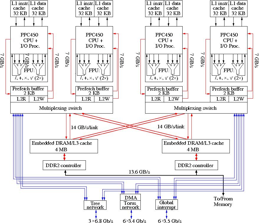
Figure 16: Block diagram of an IBM BlueGene/P processor chip.
As can be seen from the Figure the structure of the core has not changed much with respect to the BlueGene/L. The relative bandwidth from the L2 cache has been maintained: 16 B/cycle for reading and 8 B/cycle for writing. In contrast to the BlueGene/L, the cores operate in SMP mode through multiplexing switches that connect pairs of cores to the two 4 MB L3 embedded DRAM chips. So, the L3 size has doubled. Also, the memory per node has increased to 2 GB from 512 MB. Like for the BlueGene/L, the packaging and network details are discussed in section BlueGene systems.