The Cell processor, offically called the Cell Broadband Engine (Cell BE), was designed at least partly with the gaming industry in mind. Sony uses it for its PS3 gaming platform and to be successful it has to deliver high performance for the graphical part as well in doing a large amount of floating-point computation to sustain the rapidly changing scenes that occur during a game. The Cell processor is therefore not a pure graphics processor but considerably more versatile than a GPU. A testimony to this is that Mercury computers, specialised in systems for radar detection, etc., markets a product with two Cell processors, instead of dedicated DSPs (i.e., Digital Signal Processors), while Toshiba incorporates the Cell in HDTV sets and considers to bring out notebooks with a Cell processor. The Cell processor is able to operate in 32-bit as well as in 64-bit floating-point mode, though there is a large performance difference: in single precision the peak speed is 204.8 Gflop/s while in double precision it is about 14 Gflop/s. From the start there was a keen interest from the HPC community. It also restarted the discussion of the necessity of using 64-bit precision calculation all the way through an application or, by reformulation some key algorithms it would not be possible to get results with acceptable accuracy when parts would be carried out in single precision [20]. At least for the Cell processor this discussion has become of less importance as at present the variant is available under the name of PowerXCell 8i which is developed by IBM, probably expressly targeted at the HPC area. In the PowerXCell the speed for 64-bit precision has increased considerably to 102.4 Gflop/s, half the speed of the single precision computations. Also it is produced in 65 nm instead of 90 nm technology and it employs DDR2 memory instead of Rambus memory which is used in the original Cell processor. Figure 26 shows a diagram of this rather complicated processor.
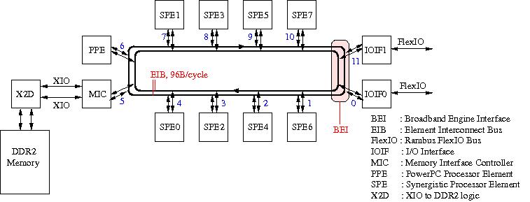
Figure 26: Block diagram of an IBM PowerXCell processor. The blue numbers in the figure indicate the device numbering used for delivering data via the Element Interconnect Bus.
As can be seen, the processor is hybrid in the sense that it contains two
different kinds of processors: The PPE, which is essentially a PowerPC core as
discussed on the PowerPC page, and 8 SPEs all running
at a clock frequency of 3.2 GHz. The SPEs are meant to do the bulk of the
computation, while the PPE takes care of operating system tasks and coordinating
the work to be done by the SPEs. All devices in the processor are connected by
the Element Interconnect Bus. The EIB in fact consists of four 16B wide rings
that transport data in opposite directions as to minimise the distance between
the devices in the processor. The devices connected to the EIB are numbered to
allow data to be transferred from one device to another can easily be delivered.
Up to 96 B/cycle can be transferred, amounting to 307.2 GB/s. Although the
PowerXCell uses DDR2 memory, the processor proper is designed for use with
Rambus memory. This has been taken care of by including the X2D device that
translates the DDR memory requests into Rambus requests and vice-versa. The two
I/O Interfaces are controlled through the Broadband Engine Interface (BEI). They
have different functions: IOIF1 takes care of the usual external I/O devices via
the IOIF protocol while IOIF0 is able to use the internal I/O protocol, BIF that
is also used on the EIB rings. In this way it is possible to connect to other
Cell processors.
The SPEs are the computational workhorses in the Cell processor. We show the
internals of an SPE in Figure 27
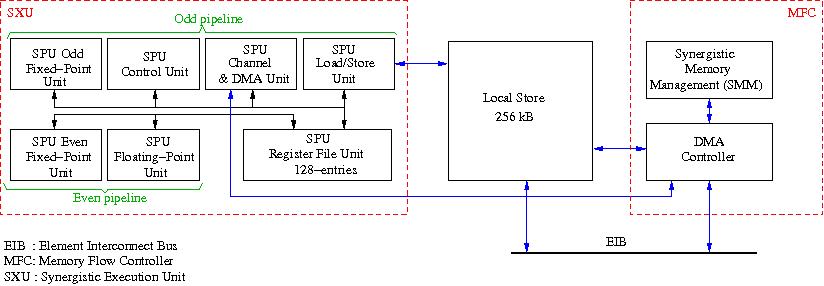
Figure 27: Block diagram of an IBM PowerXCell Synergistic Processing Element (SPE).
Roughly, there are three important parts in an SPE: the SXU (Synergistic Execution Unit) which contains the functional units for computation, load/store, and DMA-control, the Local Store that contains the local data to be operated on, and the Memory Flow Controller that in turn contains the DMA Controller and the memory management unit. As shown in Figure 27 in the SXU the functional units are organised in an odd and an even pipeline. Two instructions can be issued every cycle, one for each of these pipelines. This also implies that one floating-point instruction can be issued per cycle. Depending on type of the operands this can yield four 32-bit results or two 64-bit results per cycle (in the PowerXCell, in the original Cell processor a 64-bit result can be delivered every 13 cycles, hence the much lower double precision performance). Note that SPE does not have any form of cache. Rather, data is brought in from external memory by DMA instructions via the EIB. This leads to much lower memory latency when a data item is not in the Local Store. Up to 16 DMA requests can be outstanding for any of the SPEs. As all SPEs are independent up to 128 DMA requests can be in flight. Of course, this explicit memory management makes not for easy programming. So, one must be careful in managing the data to get (close to) optimal performance.
IBM has put much effort into a Software Development Kit for the Cell processor. It is freely available and apart from the necessary compilers, there is an extensive library for managing the data transport both from the PPE to the SPEs, between SPEs, initiating the processes on the SPEs, retrieving the results, and managing program overlays. As the Local Stores in the SPEs are small, the old concept of overlays has been revived again: The program is divided into units that depend on each other but do not constitute the whole program. By loading and unloading the units in the correct sequence one can still execute the total program. In addition, there are debugging and performance analysis tools. The total of the program development can be done using IBM's IDE, Eclipse.
The PowerXCell 8i won its share of fame for it's use in the Roadrunner system at Los Alamos National Laboratory. In this system 3240 so-called triblades are connected by InfiniBand. A triblade consists of 2 QS22 blades each containing 2 PowerXCell processors and an LS21 blade with 2 Opteron processors. This configuration was the first to break the LINPACK Petaflop barrier. This fact certainly helped in increasing the interest in the Cell processor as an accelerator platform. Presently, there are many research projects under way to assess the applicability of Cell BE accelerators and to make the learning curve for employing them effectively, less steep.