Sun has shelved its own plans to produce UltraSPARC V and VI processor by April 2004 in favour of processor designs with many (≥ 8) processor cores, each capable of handling several execution threads. This so-called Rock processor is still some time away and for the present the SPARC development in the hands of its partner Fujitsu that will advance with its own SPARC64 implementation. Both Fujitsu/Siemens and Sun market servers based on the latter processor. As Sun does not actively market its UltraSPARC IV+ based servers anymore we refrain from a description of this processor and only give details of Fujitsu's SPARC64 processor line.
For quite some time Fujitsu is making its own SPARC implementation, called SPARC64. Presently the SPARC64 is in its seventh generation, the SPARC64 VII. Obviously, the processor must be able to execute the SPARC instruction set but the processor internals are rather different from Sun's implementation. Figure 19 shows a block diagram of the quad-core SPARC64 VII.
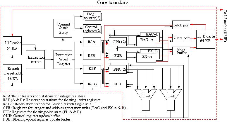
Figure 19: Block diagram of the Fujitsu SPARC64 VII processor core.
Actually, the core achitecture has not changed from the SPARC64 VI but thanks to the decrease of the feature size from 90 nm to 65 nm, now 4 cores can be placed on a chip while the highest available clock frequency is raised from 2.4 GHz to 2.52 GHz.
The L1 instruction and data caches are 64 KB, two times smaller than in the SPARC64 VI core and both 2-way set-associative. This decrease in size is somewhat surprising and probably due to the technology shrink to 65 nm feature size. There is also an Instruction Buffer (IBF) than contains up to 48 4-byte instructions and continues to feed the registers through the Instruction Word Register when an L1 I-cache miss has occurred. A maximum of four instructions can be scheduled each cycle and find their way via the reservation stations for address generation (RSA), integer execution units (RSE), and floating-point units (RSF) to the registers. The two general register files serve both the two Address Generation units EAG-A, and -B and the Integer Execution units EX-A and -B. The latter two are not equivalent: only EX-A can execute multiply and divide instructions. There also two floating-point register files (FPR), that feed the two Floating-Point units FL-A and FL-B. These units are different from those of Sun in that they are able to execute fused multiply-add instructions as is also the case in the POWER and Itanium processors. Consequently, a maximum of 4 floating-point results/cycle can be generated. In addition, FL-A and -B also perform divide and square root operations in contrast to the SPARC4+ that has a separate unit for these operations. Because of their iterative nature the divide and square root operations are not pipelined. The feedback from the execution units to the registers is decoupled by update buffers: GUB for the general registers and FUB for the floating-point registers.
The dispatch of instructions via the reservation stations,that each can hold 10 instructions, gives the opportunity of speculative dispatch: i.e., dispatching instructions of which the operands are not yet ready at the moment of dispatch but will be by the time that the instruction is actually executed. The assumption is that it results in a more even flow of instructions to the execution units.
The SPARC64 VII does not have a third level cache but on chip there is a large
(6 MB) unified L2 cache that is a 12-way set-associative write-through cache
that is shared by the 2 cores in a processor as can be seen in Figure 20. Note that the system bandwidth is the highest
available. For the lower end systems this bandwidth is about 8 GB/s.
The Memory Management Unit (not shown in Figure 19)
contains separate sets of Translation Look aside Buffers (TLB) for instructions
and for data. Each set is composed of a 32-entry µTLB and a 1024-entry
main TLB. The µTLBs are accessed by high-speed pipelines by their
respective caches.
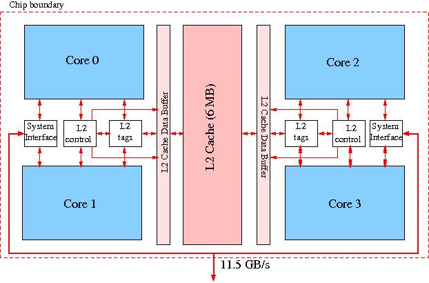
Figure 20: Block diagram of the Fujitsu SPARC64 VII processor chip. Two cores share the L2 cache.
What cannot be shown in the diagrams is that, like the IBM and Intel processors, the SPARC VII is dual-threaded per core. The type of multithreading is similar to that found in the Intel processors and is called Simultaneous Multithreading, differing from the type of multithreading present in the IBM processors but with the same name. At this moment the highest clock frequency SPARC64 available is 2.52 GHz. As already remarked, the floating-point units are capable of a fused multiply-add operation, like the POWER and Itanium processors, and so the theoretical peak performance is presently 10.08 Gflop/s/core and consequently 40.3 Gflop/s/processor.