A number of IBM systems are built from JS21 blades, the largest being the Mare Nostrum system at the Barcelona Supercomputing Centre. On these blades a variant of the large IBM PowerPC processor family is used, the PowerPC 970MP. It is a dual-core processor with a clock cycle of 2.3 GHz. A block diagram of a processor core is given in Figure8
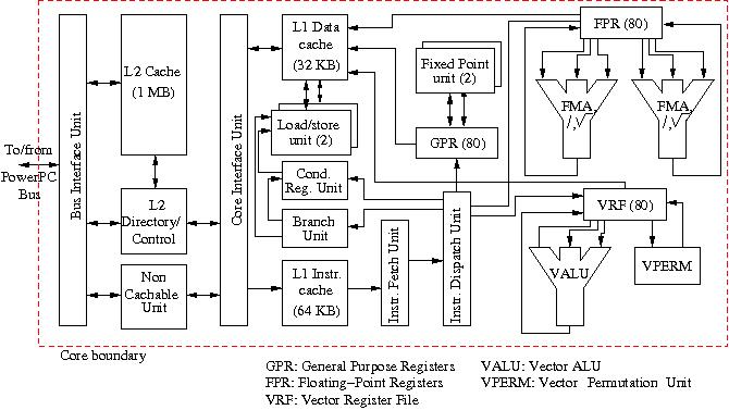
Figure 11: Block diagram of the IBM PowerPC 970 MP core.
A peculiar trait of the processor is that the L1 instruction cache is two times larger than the L1 data cache, 64 against 32 KB. This is explained partly by the fact that up to 10 instructions can be issued every cycle to the various execution units in the core. Apart from two floating-point units that perform the usual dyadic operations, there is an AltiVec vector facility with a separate 80-entry vector register file, a vector ALU that performs (fused) multiply/add operations, and a vector permutation unit that attempts to order operands such that the vector ALU is used optimally. The vector unit was designed for graphics-like operations but works quite nicely on data for other purposes as long as access is regular and the operand type agrees. Theoretically, the speed of a core can be 13.8 Gflop/s/core when both FPUs turn out the results of a fused multiply-add and the vector ALU does the same. One PowerPC 970 MP should therefore have a theoretical peak performance of 27.6 Gflop/s. The floating-point units also perform square-root and division operations.
Apart from the floating-point and vector functional units two integer fixed-point units and two load/store units are present in addition to a conditional register unit and a branch unit. The latter uses two algorithms for branch prediction that are applied according to the type of branch to be taken (or not). The success rate of the algorithms is constantly monitored. Correct branch prediction is very important for this processor as the pipelines of the functional units are quite deep: from 16 for the simplest integer operations to 25 stages in the vector ALU. So, a branch miss can be very costly. The L2 cache is integrated and has a size of 1 MB. To keep the load/store latency low, hardware-initiated prefetching from the L2 cache is possible and 8 oustanding L1 cache misses can be tolerated. The operations are dynamically scheduled and may be out-of-order. In total 215 operations may be in flight simultateously in the various functional units, also due to the deep pipelines.\\ The two cores on a chip have common arbitration logic to regulate the data traffic from and to the chip. There is no third level cache between the memory and the chip on the board housing them. This is possible because of the moderate clock cycle and the rather large L2 cache.