The Sandy Bridge processor
The current Xeon for HPC servers is the Sandy Bridge processor. A block diagram of the core is shown in Figure Figure 16.
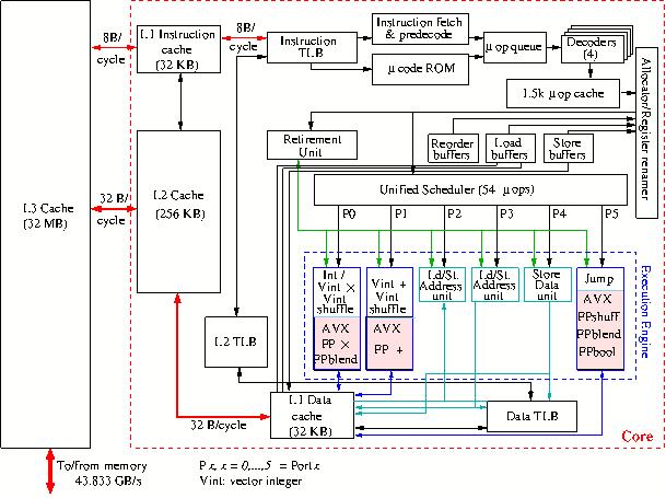
Figure 16: Block diagram of the Sandy Bridge core.
Notable differences with respect to its predecessor, the Westmere processor, are
the doubling of the bandwidth between the L1 data cache and the load buffer, the
1.5 kμ-op cache and the larger capacity of the scheduler from 32 to 54
operations. Furthermore, the vector units can perform the AVX instruction set in
256-bit wide registers. Unlike in the SSE instructions, that are still
supported, the source operands are not overwritten. So, they can be reused in
subsequent operations. Like in the Westmere processor, instructions for the
Advanced Encryption Standard (AES) are included that should speed up
en/decryption tasks. Also, like in the Westmere, the use of 1 GB pages is
supported.
To stay backwards compatible with the x86 (IA-32) Instruction Set Architecture
which comprises a CISC instruction set Intel developed a modus in which these
instructions are split in so-called micro operations (μ-ops) of fixed length
that can be treated in the way RISC processors do. In fact the μ-ops
constitute a RISC operation set. The price to be payed for this much more
efficient instruction set is an extra decoding stage. Branch prediction has been
improved and also a second level TLB cache been added.
As in the earlier Core architecture 4 μ-ops/cycle and some macro-instructions
as well as some μ-ops can be fused, resulting in less instruction handling,
easier scheduling and better instruction throughput because these fused
operations can be executed in a single cycle. As can be seen in Figure 16 the processor cores have an execution trace cache
which holds partly decoded instructions of former execution traces that can be
drawn upon, thus foregoing the instruction decode phase that might produce holes
in the instruction pipeline. The allocator dispatches the decoded instructions,
the μ-ops, to the unified reservation station that can issue up to 6
μ-ops/cycle to the execution units, collectively called the Execution Engine.
Up to 128 μ-ops can be in flight at any time. Figure
16 shows that port 0 and port 1 drive two Integer ALUs as well as
(vector) floating-point instructions. Port 5 only operates on floating-point
instructions while ports 2–4 are dedicated to load/store operations.
The two integer Arithmetic/Logical Units at port 0 and 1 are kept simple in
order to be able to run them at twice the clock speed. In addition there is an
ALU at port 1 for complex integer operations that cannot be executed within one
cycle. The length of the operands for these units is 128 bits.
A feature that cannot be shown in the figures is that the Sandy Bridge supports
multi-threading much in the style of IBM's simultaneous multithreading. Intel
calls it Hyperthreading. Hyperthreading was earlier introduced in the Pentium 4
but disappeared in later Intel processors because the performance gain was very
low. Now with a much higher bandwidth and larger caches speedups of more than
30% for some codes have been observed with Hyperthreading. Another feature that
cannot be shown is the so-called Turbo Mode already mentioned above. It means
that the clock cycle can be raised from its nominal speed (2.9 GHz for the
E5-2690) by steps of 133 MHz to up to 3.8 GHz as long as the thermal
envelope of the chip is not exceeded. So, when some cores are relatively idle
other cores can take advantage by operating at a higher clock speed.
The L3 cache is inclusive which means that it contains all data that are in the
L2 and L1 cache. The consequence is that when a data item cannot be found in the
L3 cache it is also not in any of the caches of the other cores and one
therefore need not search them.
In the Sandy Bridge processor the cores are not fully interconnected which each
other anymore but rather by two counter-rotating rings as shown in
Figure 17

Figure 17: Layout of an E5-2600 Sandy Bridge processor.
The red squares in the diagram represent the stations within the rings that
inject or draw data into/from them. The latency between stations is 1 clock
cycle. The maximum latency for updating an entry in the L3 cache is therefore
(8+2)/2=5 cycles. Although the parts of L3 cache are drawn separately in the
figure, all cores of course have access to all parts of the cache. The data only
have to be transported via the rings to the core(s) that need them.
As can be seen in the diagram there are 2 QPI links that
connect to the other CPU on the board at a bandwidth of 32 GB/s/link. The QPI
links maintain cache coherency between the caches of the CPUs. The aggregated
memory bandwidth is 51.2 GB/s over 4 channels to 1600 MHz DDR3 memory. THe I/O
unit is integrated on the chip and with one 8 GB/s and two 16 GB/s PCI3 Gen3
ports have an aggregated bandwidth of 40 GB/s.