In the systems that feature as IBM's supercomputer line, the p575 series the nodes still contain the POWER4+ chip as the computational engine although the sucessor, the POWER5+ chip already is available in other server lines of IBM. Undoubtly the POWER5 will eventually appear in the p575-like systems but presently this is not yet the case. Here we discuss the POWER5+. It should, according to IBM's official road map. be replaced quite soon by the POWER6 processor which should be fairly different from the POWER5+ but no details of the latter are available yet.
At the time of writing, the clock frequency of the POWER5+ is in the range 1.5--1.9 GHz. The POWER5+ chip it in fact a re-engineering of the POWER5 in 90 nm technology instead of 130 nm and has no really new features other than that the clock frequency might become slightly higher during its lifetime. The techonology shrink enables IBM to place two processor cores on a chip since the introduction of the POWER4 as shown in Figure 8.
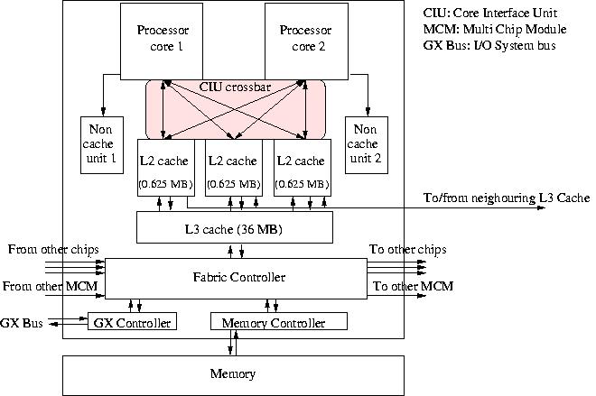
Figure 8: Diagram of the IBM POWER5+ chip layout.
At the time of writing, the clock frequency of the POWER5+ is in the range 1.5--1.9 GHz. The POWER5+ chip it in fact a re-engineering of the POWER5 in 90 nm technology instead of 130 nm and has no really new features other than that the clock frequency might become slightly higher during its lifetime. The L1 instruction cache has a size of 64 KB and is direct-mapped while the L1 data cache is 32 KB and is 4-way set associative. The chip also harbours 1.875 MB of secondary cache divided over three modules of 0.625 MB each which are 10-way set associative while the 36 MB off-chip L3 cache is 12-way set associative.
The L2 cache modules are connected to the processors by the Core Interface Unit (CIU) switch, a 2×3 crossbar with a bandwidth of 40 B/cycle per port. This enables to ship 32 B to either the L1 instruction cache or the data cache of each of the processors and to store 8 B values at the same time. Also, for each processor there is a Non-cacheable Unit that interfaces with the Fabric Controller and that takes care of non-cacheable operations. The Fabric Controller is responsible for the communication with three other chips that are embedded in the same Multi Chip Module (MCM), to L3 cache, and to other MCMs. The bandwidths at 1.9 GHz are 19.8, 13.2, and 9.9 GB/s, respectively. The chip further still contains a variety of devices: the L3 cache directory and the L3 and Memory Controller that should bring down the off-chip latency considerably, the GX Controller that responsible for the traffic on the GX bus. This bus transports data to/from the system and in practice is used for I/O or the fast communication network. Some of the integrated devices, like the Performance Monitor, and logic for error detection and logging are not shown in Figure 8. The L2 caches of two neighbouring chips are connected and the L3 caches are directly connected to the L2 caches. The L3 caches are also partitioned in three parts that each serve as a "spill cache" for their L2 counterpart, i.e., data that has to be flushed out of the L2 cache is transferrred to the corresponding L3 cache part. The L3 cache has a latency of 80 cycles as opposed to the main memory that has a latency of 220 cycles.
The better cache characteristics leads to less waiting time for regular data access: evaluation of a high order polynomial and matrix-matrix multiplication attain 90% or better of the peak performance while this is 65--75% on the POWER4+ chip. There is another feature of the POWER5+ that does not help for regular data access but which can be of benefit for programs where the data access is not so regular: Simultaneous Multithreading (SMT). The POWER5 CPUs are able to keep two process threads at work at the same time. The functional units get instructions for the functional units from any of the two threads whichever is able to fill a slot in an instruction word that will be issued to the functional units. In this way a larger fraction of the functional units can be kept busy, improving the overall efficiency. For very regular computations single thread (ST) mode may be better because in SMT mode the two threads compete for entries in the caches which may lead to trashing in the case of regular data access. Note that SMT is somewhat different from the ``normal'' way of multi-threading. In this case a thread that stalls for some reason is stopped and replaced by another process thread that is awoken at that time. Of course this takes some time that must be compensated for by the thread that has taken over. This means that the second thread must be active for a fair amount of cycles (preferably a few hundred cycles at least). SMT does not have this drawback but scheduling the instructions of both threads is quite complicated.
In many ways the POWER5+ processor core is still similar to the former POWER3 processor: there are 2 integer functional units instead of 3 (called Fixed Point Units by IBM) and instead of a fused Branch/Dispatch Unit, the POWER5+ core has a separate Branch and Conditional Register Unit, 8 execution units in all. The execution units have instruction queues associated with them that enables the out-of-order processing of up to 200 instructions in various stages. Having so many instructions simultaneously in flight calls for very sophisticated branch prediction facilities. Instructions are fetched from the Instruction Cache under control of the Instruction Fetch Address Register which in turn is influenced by the branch predict logic. This consists of a local and a global Branch History Table (BHT), each with 16 K entries and a so-called selector table which keeps track of which of the BHTs has functioned best in a particular case in order to select the prediction priority of the BHTs for similar cases coming up.
Unlike in the former POWER3, the fixed point units performs integer arithmetic operations that can complete in one cycle as well as multi-cycle operations like integer multiply and divide. There are no separate floating-point units for operations that require many cycles like divisions and square roots. All floating-point operations are taken care of in the FP units and there is an instruction to accommodate the axpy operation, called Fused Multiply Add (FMA) at IBM's which could deliver 2 floating-point results every cycle. This brings the theoretical peak performance at 7.6 Gflop/s at the current clock frequency. The composition of the floating-point operations should be such that the units have indeed enough FMAs to perform. Otherwise the performance drops by a factor of 2.
Although here the dual core version of the chip is described that is positioned for general processing, also a single core version is marketed that is recommended for HPC use. The reason is that in this case the bandwidth from the L2 cache does not have to be shared between the CPUs and a contention-free transfer of up to 108.8 GB/s can be achieved while in the dual core version a peak bandwidth of 163.2 GB/s is to be shared between both CPUs.
It is interesting to see that presently two vendors, AMD and IBM, have facilities that enable glueless coupling of processors although the packaging and implementation is somewhat different. All implementations allow for low-latency SMP nodes with a considerable number of processors stimulating the trend to build parallel systems based on SMP nodes.