


The Opteron (long known by its code name Hammer) is the newest processor from AMD and the successor of the Athlon processor. The first versions are expected to become available by the end of 2002. As it is, like the Athlon, a clone with respect to Intel's x86 Instruction Set Architecture, it will undoubtly frequently be used used in clusters. Therefore we discuss this processor here although it is not used presently in integrated parallel systems.
The Opteron processor has many features that are also present in modern RISC processors: it supports out-of-order execution, has multiple floating-point units, and can issue up to 9 instructions simultaneously. In fact, the processor core in very similar to that of the Athlon processor. A block diagram of the processor is shown in Figure 7
It shows that the processor has three pairs of Integer Execution Units
and Address Generation Units that via an 24-entry Integer Scheduler
takes care of the integer computations and address calculations. Both
the Integer Scheduler and the Floating-Point Scheduler are fed by the
96-entry Instruction Control Unit that receives the decoded
instructions from the instruction decoders. An interesting feature of
the Opteron is the pre-decoding of x86 instructions in fixed-length
macro-operations, called RISC Operations (ROPs), that can be stored in
a Pre-decode Cache. This enables a faster and more constant instruction
flow to the instruction decoders. Like in RISC processors, there is a
Branch Prediction Table assisting in branch prediction.
The floating-point units allow out-of-order execution of instructions
via the FPU Stack Map & Rename unit. It receives the floating-point
instructions from the Instruction Control Unit and reorders them if
necessary before handing them over to the FPU Scheduler. The
Floating-Point Register File is 88 elements deep which approaches the
number of registers as is available on RISC processors.
(For the x86 instructions 16 registers in a flat register file are
present instead of the register stack that is usual for Intel
architectures.)
The floating-point part of the processor contains three units: a
Floating Store unit that stores results to the Load/Store Queue Unit
and Floating Add and Multiply units that can work in superscalar mode,
resulting in two floating-point results per clock cycle. Because of the
compatibility with Intel's Pentium III processors, the floating-point
units also are able to execute Intel MMX instructions and AMD's own
3DNow! instructions. However, there is the general problem that such
instructions are not accessible from higher level languages, like
Fortran 90 or C(++). Both instruction sets are meant for massive
processing of visualisation data and only allow for 32-bit precision to
be used.
Due to the shrinkage of components the chip now can harbour the
secondary cache of 256 KB and the memory controller. This, together
with a significantly enhanced memory bus can deliver up to 5.3 GB/s of
bandwidth, an enormous improvement over the former memory system. This
memory bus, called HyperTransport by AMD, is derived from licensed
Compaq technology and similar to that employed in Compaq's EV7
processors (see the Compaq Alpha EV7). It
allows for "glueless" connection of several processors to form
multi-processor systems with very low memory latencies.
The clock frequency will be in the order of 2 GHz of the current processors
the Opteron is an interesting alternative for many of the RISC processors
that are available at this moment. Especially the HyperTransport
interconnection possibilities could be highly interesting for building
SMP-type clusters.
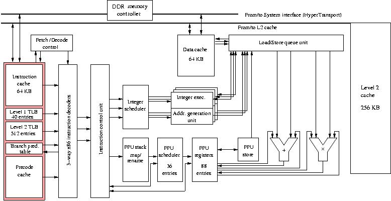
Figure 7: Block diagram of AMD Opteron processor.
Next:
Compaq Alpha EV7
Up:
The Main Architectural Classes
Previous:
Processors