


The present CPU that is employed in Compaq machines like the AlhpaServerSC and the Wildfire and in various cluster systems is the Alpha EV68 processor. Shortly, (second half 2002) EV7 processors will become available. Because of the EV7 structure the macro-architecture of these systems may also significantly change (see below). The core of the EV7 processor is almost identical to that of the EV68 architecture and is depicted in Figure 8a
A notable fact is that there are two duplicate integer register
files both with 80 entries, that each service a set of integer
functional units called cluster 0 and cluster 1, respectively, by
Compaq. The four integer Add/Logical units can exchange values in one
cycle if required. Although this is not shown in the diagram, the
integer multiply is fully pipelined. The two integer clusters and the
two floating-point units enable the issueing of up to 6 instructions
simultaneously. The two load/store units draw on a 64 KB instruction
and a 64 KB data cache that are both 2-way set-associative. Four
instructions can be accepted for (speculative) processing. Of the 80
integer and 72 floating-point registers 41 in both register files can
hold speculative results. The out-of-order issueing of instructions is
supported via an integer queue of length 20 and a floating-point queue
with 15 entries. However, as the integer processing clusters do not
contain the same functional units, the issueing of integer instructions
cannot all be scheduled dynamically. Those instructions that need to
execute in a particular unit (e.g., an integer multiply that is only
available in cluster 0) are scheduled statically. As soon as an
instruction is issued or is terminated due to mis-speculation it is
removed from the queue and can be replaced by another instruction.
Instruction fetching is governed by the branch predictor. This hardware
contains global and local prediction tables and Branch History Tables
(BHTs) to train the predictor in order to obtain an optimal instruction
fetch to the instruction cache and registers.
The feature density used is 0.18 µm instead of 0.25 µm which
enables the location of a 1.5 MB secondary cache and 2 memory controllers
on chip. The largest difference will be that there will be 4 dual
channels (North, East, South, West) from the chip to interconnect it with
neighouring chips at a bandwidth of 1.6 GB/s per single channel for what
Compaq calls "seamless SMP processing" and is, as the name suggests,
well-suited to build SMP nodes with low memory latency. The layout of
the complete chip is shown in Figure 8b
The path to memory is implemented by 4×5 RAMBUS links as the
systems will be fitted with RAMBUS memory yielding a bandwidth of 6 GB/s.
The direct I/O dual link from the chip also has a bandwidth of 1.6 GB/s.
The chip is expected to ship first at a clock frequency of 1--1.2 GHz.
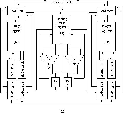
Figure 8a: Block diagram showing the functional units in an
Alpha EV7 processor.
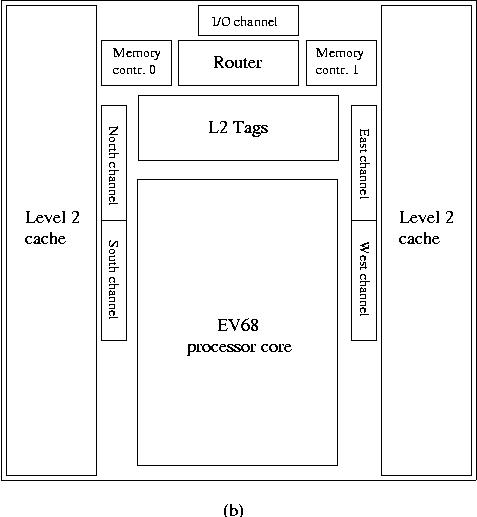
Figure 8b:
Chip layout for the Alpha EV7 processor.
Next:
Hewlett Packard PA-RISC 8700
Up:
The Main Architectural Classes
Previous:
AMD Opteron
Aad van der Steen
Mon Jul 29 12:27:40 MDT 2002