


The UltraSPARC-III is the third generation from the UltraSPARC family and, as one of the last RISC processor families, with full 64-bit precision and addressing range. It is built in 0.18 µm CMOS technology at a clock frequency that is currently 900 MHz. It is a complete revamp of earlier UltraSPARC designs but backward compatible with these older processors. UltraSPARCs are used in all SUN products from workstations to the heavy E10000 servers and also in Fujitsu products like the AP-3000. We show a block diagram of the UltraSPARC-III in Figure 14.
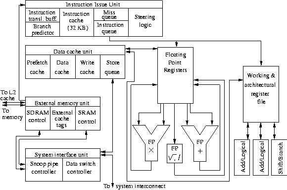
Figure 14: Block diagram of the UltraSPARC III processor.
The chip is characterised by large large amount of caches of various
sorts as can be seen in the figure. The Data Cache Unit (DCU) contains
apart from a 4-way set associative cache of 64 KB also a write and a
pre-fetch cache, both of 2 KB. The pre-fetch cache is independent from
the data cache and can load data when this is deemed appropriate. The
write cache defers writes to the L2 cache and so may evade unnecessary
writes of individual bytes until entire cache lines have to be
updated. The Instruction Issue Unit (IIU) contains the 32 KB 4-way set
associative instruction cache together with the instruction TLB which
is called Instruction translation buffer in SUN's terminology. The IIU
also contains a so-called miss queue that holds instructions that are
immediately available for the execute units when a branch has been
mis-predicted. Branch prediction is fully static in the
UltraSPARC-III. It is implemented as a 16 KB table in the IIU that is
pipelined because of its size.
The Integer Execute Unit (IEU) has two Add/Logical Units and a branch
unit. Integer adds and multiplies are pipelined but the divide
operation is not. It is performed by an Arithmetic Special Unit (not
shown in the figure) that does not burden the pipelines for the ALUs.
The integer register file is effectively divided in two and is called
the Working and Architectural Register File by SUN. Operands are
accessed and results stored in the working registers. When an exception
occurs, the results to be undone in the working registers are overwritten
by those from the architectural file.
The floating-point unit (FPU) has two independent pipelined units for
addition and multiplication and a non-pipelined unit for floating
division and square-root computation that require in the order of
20--25 cycles. The FPU also contains graphics hardware (not shown in
Figure 14) that shares the pipelined adder
and multiplier with general 64-bit calculations. For the chips
delivered at 1050 MHz, the theoretical peak performance is 2.1 Gflop/s.
It is expected that the UltraSPARC-III technology can be shrunk to
reach a clock frequency that is slightly more by the end of its life cycle.
The size of the L2 cache can be up to 8 MB.
The memory controller and the L2 cache controller together with the L2
cache tags are all housed on the chip in the External Memory Unit. This
shortens the latency of accesses from both memory levels. In addition,
both controllers communicate with the System Interface Unit (SIU), also
on-chip to keep in touch with the snoop pipe controller in the SIU. The
processor has been built with multi-processing in mind and the snoop
controller keeps track of data requests in the whole system to ensure
coherency of the caches when required.
The UltraSPARC-III is around for about a more than 2 years at the time of
writing and the clock frequency has gone up in that period from 750 to 1050
MHz. The next generation UltraSPARC IV should appear somewhere in 2004. After
the radical redesign in the present generation, it will have most of the same
characteristics as the current one apart from larger caches, etc.